All over the world, force transducers are usually produced with glued strain gauges. We at Primosensor always doublecheck whether the customer’s requirements can be fulfilled better by using thin or thick film technology.
In thin film technology, strain-sensitive materials are condensed onto the metal surface of the sensor via PVD (sputtering) and eventually structured using photolithography, making extremely precise circuit structures possible. Moreover, thin film technology allows us not to use organic glue if it would interfere with the setup (radioactive radiation).
Coating force sensors directly is only cost-effective if the sensor is small enough, as the price for coating increases in proportion to the area to be coated. Higher nominal loads require a bigger sensor body. We therefore need a different approach to cost-effectively use thin film technology in force sensor technology.
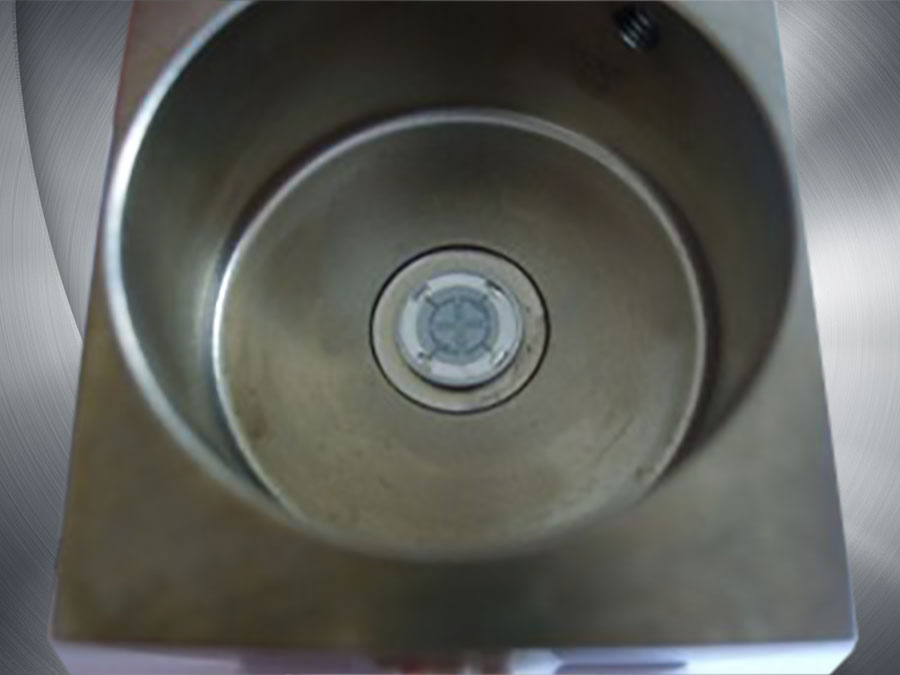
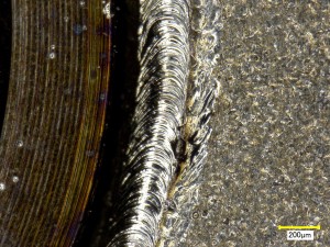
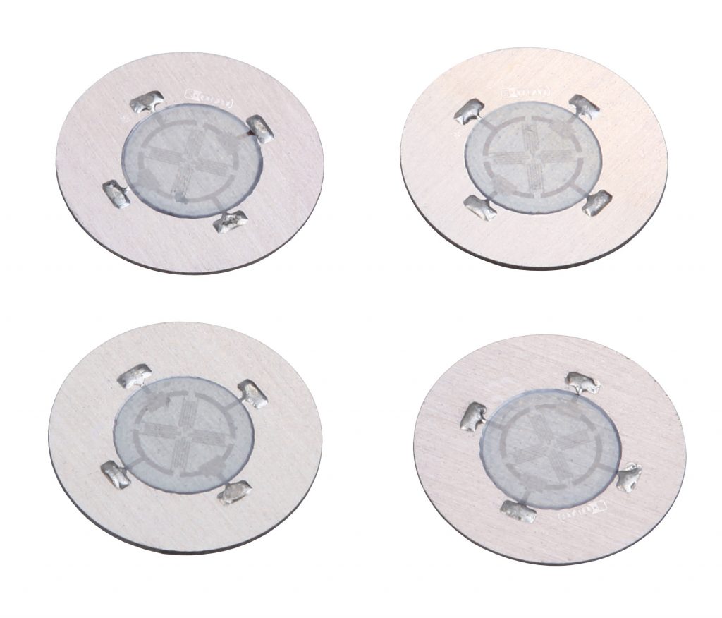
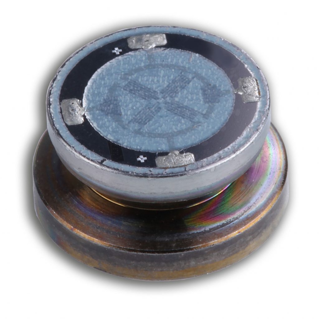
The solution is to produce small thin film sensor elements on sheets and in high quantities, to reduce the price per piece. Each sensor element is equipped with a Wheatstone full bridge and welded on or into the deformable body, depending on their geometrical form, which is either plates or pots. Elaborated process monitoring ensures our products’ high quality.
In the future, highly sensitive layers will enable us to implement huge overload strengths or very small nominal loads in force transducers.
Profitability of thin film technology
Producing circular blanks on sheets and by thin film technology improves profitability.